Wedoany.com Report-Mar 13, Solar microgrid-powered PairTreeA Chinese research team has successfully developed a single-atom-thick metal layer, with a thickness just one two-hundred-thousandth of a human hair's diameter, achieving the world's first large-area production of two-dimensional (2D) metal materials.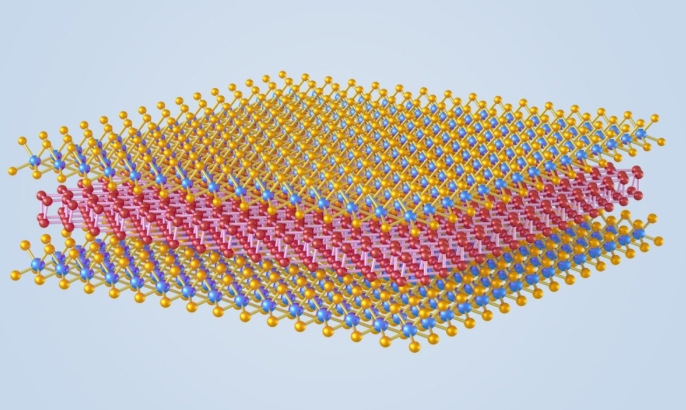
Single-layer bismuth encapsulated by single-layer molybdenum disulfide Photo: Courtesy of the Institute of Physics of the Chinese Academy of Sciences
This innovative material, developed by researchers at the Institute of Physics (IOP) of the Chinese Academy of Sciences, opens up a new frontier in 2D metal research, and it holds the potential to revolutionize technologies such as ultra-small, low-power transistors and transparent displays, the research team said.
"This marks the first successful fabrication of large-area 2D metal materials. Moreover, previously, small-scale thin metal layers were highly unstable. For the first time, we have achieved environmentally stable 2D materials, which show no performance degradation even after a year," .
These 2D metals are just one-millionth the thickness of an A4 sheet of paper and one two-hundred-thousandth the diameter of a human hair, according to the research team.
In the scientific community, genuine 2D materials are defined as those with a thickness of one or a few atoms. However, achieving such thinness with metal materials has long been a significant scientific challenge.
Led by Zhang Guangyu, the research team developed an atomic-level manufacturing technique called van der Waals (vdW) squeezing. This method uses a specially designed anvil made of atomically flat materials with no dangling bonds on its surface.
The team introduced that they melted metals and used high-quality single-layer molybdenum disulfide (MoS₂) vdW anvils, which they had previously prepared, to squeeze the metals. This process enabled the consistent fabrication of 2D metals such as bismuth, tin and lead at the atomic thickness limit.
"This breakthrough is expected to usher in a new era in 2D metal studies, paving the way for further technological advancements in areas such as ultra-miniature low-power transistors, high-frequency devices, transparent displays, ultra-sensitive sensors and highly efficient catalysis, among other fields, " Zhang noted.
"Moreover, the vdW squeezing technique has opened up an effective atomic-level manufacturing pathway for 2D metal alloys, amorphous materials, and other non-layered 2D materials, painting a promising vision for a wide range of emerging quantum, electronic and photonic device applications," Zhang added.
The realization of 2D metals at the atomic thickness limit goes beyond the current vdW layered material systems, filling a critical gap in the 2D material family, said Du Luojun, another researcher at the IOP.